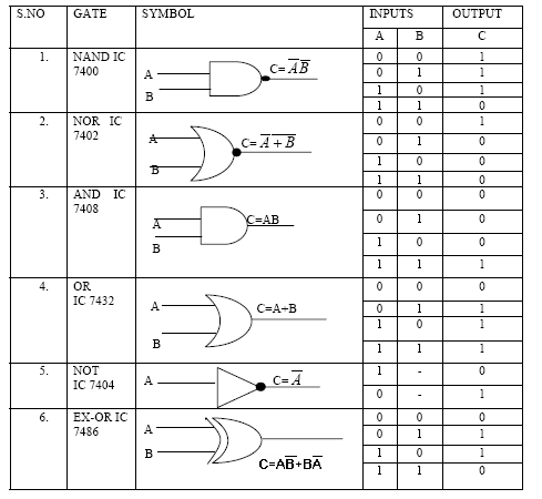
Study and analyze standard digital ICs
Prerequisite:
- Study about digital logic gates, symbols and truth tables.
- Study about universal logic gates and realization of basic gates using universal gates.
- Study the procedure for conducting the experiment in the lab.
Objectives:
- Study of logic gates using IC’s.
- Study of flip-flops using ICs
Apparatus:
| IC 7400, IC 7404, IC 7408, IC 7432, IC 7486 | 1No. each |
| Flip-flop ICs – 7474, 7476 | 1No. each |
| Connecting patch chords | |
| IC Trainer Kit |
Theory:
A logic gate performs a logical operation on one or more logic inputs and produces a single logic output. The logic is normally performed as Boolean logic and is most commonly found in digital circuits.
The different types of logic gates are:
- NOT gate
- OR gate
- AND gate
- EX-OR gate
- NAND gate
- NOR gate
Inverter or NOT gate: The inverter is a logic gate which has only one input & one output. In inverter a low input produces a high output and a high input produces a low output.
Logic equation is: 
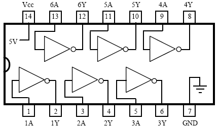
Digital IC for NOT: IC 7404
AND gate: AND gate is a logic gate which can have two or more inputs. But there is only one output. The output of AND gate is high only if all inputs are high. Even if one input is low, the output will be low.
Logic equation is: Y = AB
Digital IC for AND: IC 7408
OR gate: An OR gate is a logic gate which can have two or more inputs and a single output. The output of an OR gate is high if any of the inputs or all inputs are high. The output is low only if all the inputs are low.
Logic equation is: Y = A + B
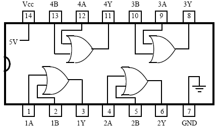
Digital IC for OR: IC 7432
NAND gate: NAND gate is a combination of AND & NOT gates. Thus NAND gate is the inverse of AND gate. The output is low when all inputs are high. The output is high for all the remaining combinations.
Logic equation is: 
Digital IC for NAND: IC 7400
NOR gate: NOR gate is a combination of OR & NOT gates. Thus NOR gate is the inverse of OR gate. When all or either of the inputs are high output is low. The output of NOR gate is high only when all inputs are low.
Logic equation is: 
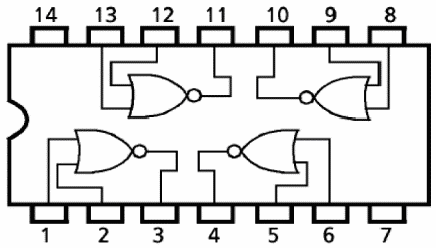
Digital IC for NOR: IC 7402
EX-OR gate: In EX-OR gate if either of the inputs is high, output will be high. If both the inputs are high output will be low. If both inputs are low then also output will be low.
Logic equation is: 
Digital IC for EX-OR: IC 7486
Table. 5.1 Logic gates symbols and truth tables
Circuit Diagrams:
 |
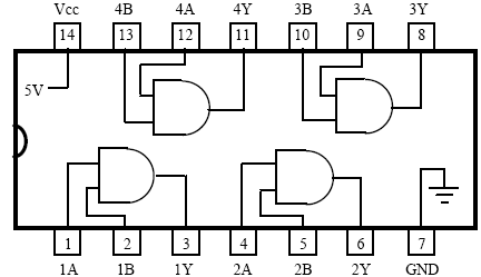 |
| Fig 5.1 NOT gate (IC 7404) | Fig 5.2 AND gate (IC 7408) |
 |
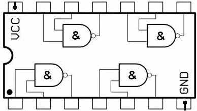 |
| Fig 5.3 OR gate (IC 7432) | Fig 5.4 NAND gate (IC 7400) |
 |
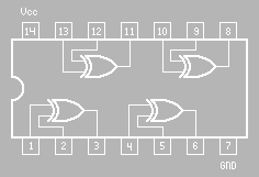 |
| Fig 5.5 NOR gate (IC 7402) | Fig 5.6 EX-OR gate (IC 7486) |
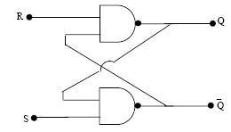
SR FIip-FIop:
The fundamental latch is the simple SR flip-flop, where S and R stand for set and reset respectively. It can be constructed from a pair of cross-coupled NOR logic gates. The stored bit is present on the output marked Q.
Normally, in storage mode, the S and R inputs are both low, and feedback maintains the outputs in a constant state, with Q and the complement of Q. If S (Set) is given with high while R is held low, then the Q output is forced high, and stays high even after S returns low; similarly, if R (Reset) is given with high while S is held low, then the Q output is forced low, and stays low even after R returns low.
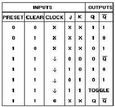
JK FIip-FIop:
The JK flip-flop augments the behavior of the SR flip-flop (J = Set, K = Reset) by interpreting the S = R = 1 condition as a “flip“ or toggle command. Specifically, the combination J = 1, K = 0 is a command to set the flip-flop; the combination J = 0, K = 1 is a command to reset the flip-flop; and the combination J = K = 1 is a command to toggle the flip-flop, i.e., change its output to the logical complement of its current value.
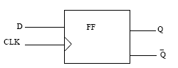
D FIip-FIop:
The Q output always takes on the state of the D input at the moment of a rising clock edge. (or falling edge if the clock input is active low) It is called the D flip-flop for this reason, since the output takes the value of the D input or Data input, and Delays it by one clock count. The D flip-flop can be interpreted as a primitive memory cell, zero-order hold, or delay line.
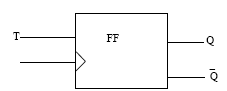
T FIip-FIop:
If the T input is high, the T flip-flop changes state (“toggles“) whenever the clock input is strobed. If the T input is low, the flip-flop holds the previous value. This behavior is described by the characteristic equation: A T flip-flop can also be built using a JK flip-flop (J & K pins are connected together and act as T) or D flip-flop.
Circuit Diagrams and Truth Tables:
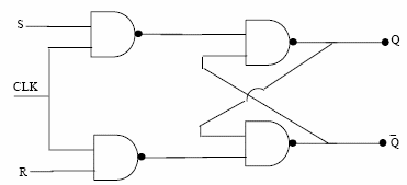
RS FIip-FIop:
 |
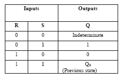 |
Fig. 6.1 RS Flip-Flop basic version
 |
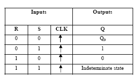 |
Fig. 6.2 RS Flip-Flop Clocked version
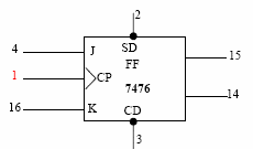
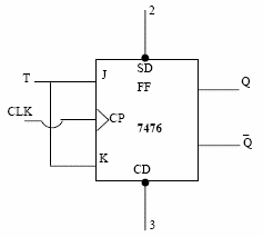
JK FIip-FIop:
Symbol:
 |
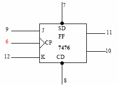 |
Fig. 6.3 JK Flip-Flop using IC 7476
(Power connection, ground connection, the above are two JK Flip-Flops in a single IC)
Truth table:
D FIip-FIop using JK FIip-FIop:
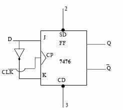 |
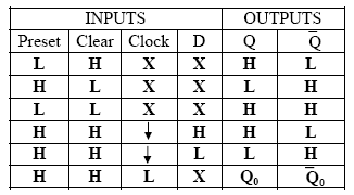 |
Fig. 6.4 D-Flip-Flop using JK Flip-Flop & its Truth table
Symbol:
T FIip-FIop using JK FIip-FIop:
 |
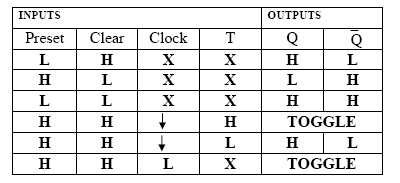 |
Fig. 6.5 T-Flip-Flop using JK Flip-Flop & its Truth table
Symbol:
Procedure:
- Connect the NOT gate using digital IC’s as shown in the figure 5.1.
- Use +5V for logic l and 0V for logic 0.
- Feed the logic signals 0 or l from the logic input switches at the inputs A & B.
- Monitor the output using LED indicators and verify its truth table.
- Repeat step l to 4 for all the remaining gates.
Procedure:
- Construct the RS flip flop as shown in figures 6.1 & 6.2
- Feed the logic signals from the logic input switches observe the logic outputs on the logic Level LED indicators.
- Verify the corresponding truth tables.
- Construct JK - flip flop (fig 6.3) and repeat step2 and 3.
- Construct D - flip flop (fig 6.4) and repeat step 2 and 3.
- Construct T - flip flop (fig 6.5) and repeat step 2 and 3.
Inference:
Different types of logic gates and Flip flops (RS, Clocked RS, JK, D, T) are constructed using IC 7476 and hence their truth tables are verified.
Design Experiments:
Design Experiment: 1
Band pass filter using 741 IC. (ICA Lab)
By connecting low pass Filter and High pass filter in series, Band pass filter is achieved. Please refer experiment No. 3 above for other details.
Open Experiment: 1
Applications of Op-Amp:
Aim: To study the application of op-amp like Voltage to current converters, current to voltage converters, Log amplifiers, anti-log amplifiers etc.
References:
- D. Roy Choudhury and Shail B.Jain, Linear Integrated Circuits, 2nd edition, New Age International
- Ramakant A. Gayakwad, Operational and Linear Integrated Circuits, 4th edition, PHI
- S. Franco, Design with Operational Amplifiers and Analog Integrated Circuits, 3rd edition, TMH.
- James M. Fiore, Operational Amplifiers and Linear Integrated Circuits: Theory and Application, WEST.
- J.Milliman and H.Taub, Pulse and digital circuits, McGraw-Hill.
- David A. Bell, Solid State Pulse circuits, PHI .
- Roy Mancini, OPAMPs for Everyone, 2nd edition, Newnes.
- Anand Kumar, Pulse and Digital Circuits, PHI .
- William D. Stanley, Operational Amplifiers with Linear Integrated Circuits, 4th edition, Pearson.
- www.analog.com
- www.datasheetarchive.com
- www.ti.com
-
UpdatedOct 26, 2016
-
Views11,480