Measrement of IC741 Op-Amp parameters
Prerequisite:
- Pin out of IC 741C with supply voltage rejection ratio.
- Immense knowledge of Op-Amp’s AC and DC characteristics.
Objective:
- To study the pin configurations, specifications & functioning of IC 741 Op-Amp.
- To measure the Op-Amp parameters and compare them with ideal characteristics.
Apparatus:
- IC µA 741 OP-Amp.
- CRO.
- Dual Regulated Power Supply
- Voltmeter 0-10mV - 2 Nos.
- Ammeters 0-10 µA - 2 Nos.
- Connecting Wires.
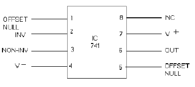
Pinout and Circuit diagrams:
IC µA741 OP-AMP
Specifications:
| Supply voltage | |
| µA 741A, µA 741, µA 741E | ± 22V |
| µA 741C | ± 18V |
| Internal power dissipation | |
| DIP package | 310 mw |
| Differential input voltage | ± 30V |
| Operating temperature range | |
| Military (µA 741A, µA 741) | -550 to +1250 C |
| Commercial (µA 741E, µA 741C) | 00 C to +700 C |
| Input offset voltage | 1.0 mV |
| Input Bias current | 80 nA |
| PSSR | 30µV/V |
| Input resistance | 2MΩ |
| CMMR | 90dB |
| Output resistance | 75Ω |
| Bandwidth | 1.0 MHz |
| Slew rate | 0.5 V/µ sec |
Circuit Diagrams:
a) Input bias current and input offset current
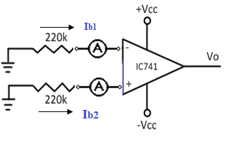
Figure 1.
Input Bias current: (Ib1 + Ib2) / 2
Input offset current: |Ib1 - Ib2|
b) Input offset voltage
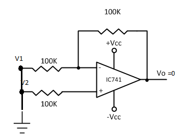
Figure 2.
Viof = The input voltage for which the output Vo is zero. Otherwise, it is the output voltage for input zero with unit gain amplification.
c) CMRR (Common Mode Rejection Ratio)
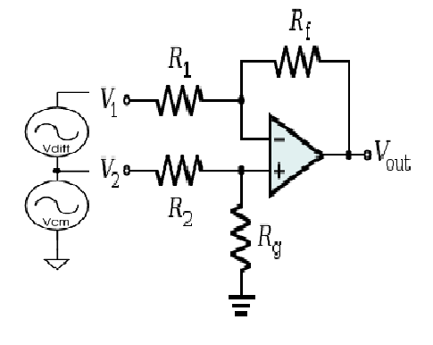
Figure 3.
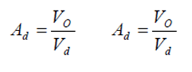
CMRR = Ad / Ac, Differential input voltage is given between V1 and V2 and common mode voltage is given as common to both the inputs.
d) PSRR (Power supply Rejection Ratio)
The variation of the output voltage due to variation of the power given to the IC. It is measured as µV / V.
e) Slew rate and Bandwidth
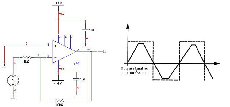
Figure 4.
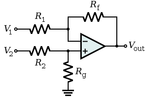
Figure 5.
Theory:
An op-amp is a high gain, direct coupled differential linear amplifier choose response characteristics are externally controlled by negative feedback from the output to input, op-amp has very high input impedance, typically a few mega ohms and low output impedance, less than 100Ω.
Op-amps can perform mathematical operations like summation integration, differentiation, logarithm, anti-logarithm, etc., and hence the name operational amplifier op-amps are also used as video and audio amplifiers, oscillators and so on, in communication electronics, in instrumentation and control, in medical electronics, etc.
Op-Amp characteristics:
An ideal op-amp draws no current from the source and its response is also independent of temperature. However, a real op-amp does not work this way. Current is taken from the source into op-amp inputs. Also the two inputs respond differently to current and voltage due to mismatch in transistors. A real op-amp also shifts its operation with temperature. These non-ideal characteristics are:
- Input bias current
- Input offset current
- Input offset voltage
- Thermal drift
- Slew rate
- Input and output voltage ranges
Procedure:
- Connect the IC 741 with supply voltages on a bread board.
- Connect the CRO as per the requirement for voltage and for current measurement.
- Measure the parameters of Op-Amp and compare them with ideal one.
1. Input bias current and input offset current:
- Connect the circuit as shown in figure for Input bias current and input offset current.
- Measure the current at inverting and non inverting terminals of op-amp as IB+ and IB-.
- Average these values to find out the input Bias current. Also, find the difference between these two currents to know the input offset current.
| IB+ | IB- | Input Bias Current | Input Offset Current |
|---|---|---|---|
2. Input offset voltage:
- Connect the circuit as shown in Figure 2. for Input offset voltage measurement.
- Give zero volts as input and measure the output.
| Output Voltage (Vout) | Input Voltage at Inverting Terminal V1(V) | Input Voltage at Non-Inverting Terminal V2(V) |
|---|---|---|
3. Slew Rate:
- Connect the circuit diagram as shown in figure 4.
- Apply A square wave of low frequency at inverting terminal of op-amp.
- The input amplitude of square wave is to be adjusted until the output is 20 volts peak to peak.
- The frequency is then to be adjusted until the output becomes triangular.
- The rising edge slope of the triangle-wave was taken to be the slew rate that was being sought.
| Input Voltage at Inverting Terminal V(V) | Output Slope V/µ Sec | Frequency (Hz) |
|---|---|---|
4. CMRR Measurement:
Configure the Op-Amp in unit gain configuration, in differential mode operation as shown in figure 3.. Give 1V as differential input and observe the output as 1V. Keeping the differential input same as 1V, increase the common mode voltage from 0V to 10V insteps of 1V and observe the variation in the output. Calculate Ad and Ac and CMRR.
5. Bandwidth:
Connect the op-amp in unit gain configuration as shown in figure 5. Apply 1V sinusoidal input at 10Hz and observe the output. Increase the frequency in steps (semi-logarithemic scale) and note the output voltage values. Identify the -3dB cut-off point, which gives the band width.
Result:
The pin configuration, specifications & functioning of different integrated circuits used in the practical applications have been studied.
-
UpdatedOct 24, 2016
-
Views15,273