HDL code to realize all the logic gates
Prerequisites: Study of the functionality of logic gates.
Objective: To design all types the logic gates using Verilog HDL Programming and verify their simulation and synthesis reports.
Software and Hardware: Xilinx ISE 9.2i and FPGA Spartan-3E.
Theory:
A logic gate performs a logical operation on one or more logic inputs and produces a single logic output. The logic is normally performed as Boolean logic and is most commonly found in digital circuits.
The different types of logic gates are:
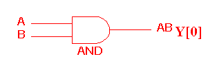
i. AND gate
 |
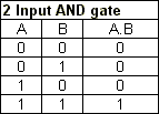 |
The AND gate is an electronic circuit that gives a high output (1) only if all its inputs are high. A dot (.) is used to show the AND operation i.e. A.B. Bear in mind that this dot is sometimes omitted i.e. AB
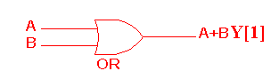
ii. OR gate
 |
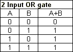 |
The OR gate is an electronic circuit that gives a high output (1) if one or more of its inputs are high. A plus (+) is used to show the OR operation.
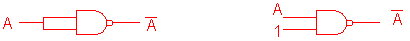
iii. NOT gate
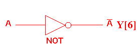 |
 |
The NOT gate is an electronic circuit that produces an inverted version of the input at its output. It is also known as an inverter. If the input variable is A, the inverted output is known as NOT A. This is also shown as A', or A with a bar over the top, as shown at the outputs. The diagrams below show two ways that the NAND logic gate can be configured to produce a NOT gate. It can also be done using NOR logic gates in the same way.
iv. NAND gate
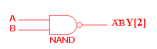 |
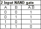 |
This is a NOT-AND gate which is equal to an AND gate followed by a NOT gate. The outputs of all NAND gates are high if any of the inputs are low. The symbol is an AND gate with a small circle on the output. The small circle represents inversion.
v. NOR gate
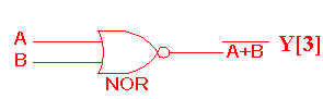 |
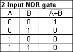 |
This is a NOT-OR gate which is equal to an OR gate followed by a NOT gate. The outputs of all NOR gates are low if any of the inputs are high.
The symbol is an OR gate with a small circle on the output. The small circle represents inversion.
vi. EXOR gate
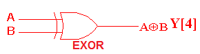 |
 |
The 'Exclusive-OR' gate is a circuit which will give a high output if either, but not both, of its two inputs are high. An encircled plus sign () is used to show the EOR operation.
vii. EXNOR gate
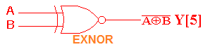 |
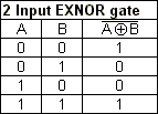 |
The 'Exclusive-NOR' gate circuit does the opposite to the EOR gate. It will give a low output if either, but not both, of its two inputs are high. The symbol is an EXOR gate with a small circle on the output. The small circle represents inversion.
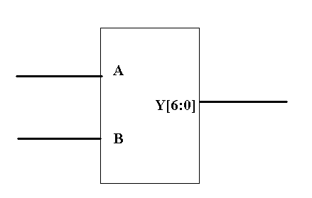
Block Diagram:
Verilog Code:
module basicgates(Y,A,B);
    input A,B;
    output [6:0] Y;

    and g1(Y[0],A,B);
    or g2(Y[1],A,B);
    nand g3(Y[2],A,B);
    nor g4(Y[3],A,B);
    xor g5(Y[4],A,B);
    xnor g6(Y[5],A,B);
    not g7(Y[6],A);

endmodule
Test Bench Code:
module gatetest_v;
// Inputs
reg A;
reg B;
// Outputs
wire [6:0] Y;
// Instantiate the Unit Under Test (UUT)
gates uut(
.Y(Y),
.A(A),
.B(B)
);
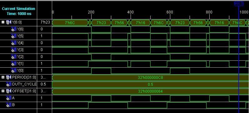
initial begin
A = 0; B = 0; #20;
A = 0; B = 1; #20;
A = 1; B = 0; #20;
A = 1; B = 1; #20;
end
endmodule
Simulation Results:
Result: Designed and verified logic gates using Verilog VHDL.
Learning Outcome: After completion of this experiment, students are able to design logic gates using Verilog VHDL.
Viva Questions:
- What is the full form of VHDL?
- What are the advantages of verilog HDL?
- Design Ex-OR gate using behavioral model?
- What are the universal gates? Why they are called so?
- What are the advantages of minimizing the logical expressions?
- What does a combinational circuit mean?
- Implement EXOR gate using NOR gates.
-
UpdatedOct 30, 2016
-
Views12,705