Schmitt Trigger
Prior to the Lab session:
1. Study the operation and working principle of Schmitt Trigger.
2. Study the procedure for conducting the experiment in the lab.
Objectives:
1. To design the circuit of Schmitt trigger with UTP=2.2V and LTP=1V.
2. To obtain square wave from sine wave.
3. To obtain UTP and LTP values practically
Apparatus:
1. CRO 0-20 MHz (Dual channel) - 1No.
2. Function generator 0- 1MHz - 1No.
3. Capacitor (0.1µF) - 1 No.
4. Resistors (1kohms, 2.2Kohms, 330ohms - 1 No. each
5. Resistor (1.2 Kohms - 3 No.
6. Transistor (BC 107) - 2 No.
7. Regulated Power supply 0-30 V (dual ) - 1 No.
8. Connecting wires
9. Bread board
Circuit diagram:
Theory:
In digital circuits fast waveforms are required i.e, the circuit remain in the active region for a very short time (of the order of nano seconds) to eliminate the effects of noise or undesired parasitic oscillations causing malfunctions of the circuit. Also if the rise time of the input waveform is long, it requires a large coupling capacitor. Therefore circuits which can convert a slow changing waveform (long rise time) in to a fast changing waveform (small rise time) are required. The circuit which performs this operation is known as “Schmitt Trigger”.
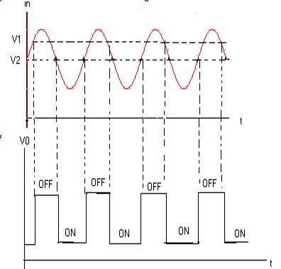
In Schmitt trigger circuit, the output is in one of the two levels namely low or high. When the input voltage is raising above the UTP (upper threshold point) i.e. V1, the output changes to high level. Similarly when a falling output voltage passes through a voltage V2 known as lower threshold point (LTP), the output changes to low. The level of the output changes V1 is always greater than V2.The differences of these two voltages is known as “Hysteresis”.
Design Procedure:
The voltage required to drive the transistor Q1 from OFF to ON is called upper trigger point.
UTP = V1 = V1 — 0.1
Where V1 = V = ( VCCR2)/ (R1+R2+RC1)
The voltage required to drive the transistor Q1 from ON to OFF is called lower trigger point.
LTP = V2= VBE(active)+ (V1-V?2) .Re/(aRcth+Re)
Where Rcth =(RC1(R1+R2))/( R1+R2+RC1) a =R2/(R1+R2)
Choose BC107 transistor with hfe= 200
Let Vcc=12V, R1=2.2Kohms , R2=1.2Kohms
Set UTP = V1 — 0.1 then 2.2= V1 — 0.1 then V1= 2.3V
But V1= (12X15)/(2.2+1.5+RC1) RC1= 4.12Kohms = 4Kohms
Rcth = (4X 10³(2.2+1.5))/(2.1+1.2+4.4K) = 1.97Kohms
a= 0.3529
LTP =V2= VBE(active)+ (V1-V?2) .Re/(aRcth+Re)
= 0.7+(2.3-0.6).330/(0.35X1.97K+330)
= 1.21V
VE=V1-VBE= 2.3-0.7 = 1.6V
IB2= VE/RE(1+hfe) = 1.6/330(1+200) = 0.0030A
IC2 = hfeIB2 =0.6V
When Vin < V2, output =1
(VC-output)/IC2 = RC2 ---------> (12-1)/0.6 = RC2= 18.33%u2126
Procedure:
1. Connect the circuit diagram as shown in circuit diagram.
2. Apply a sine wave input of 15 Vp-p amplitude and 1 KHz frequency to the circuit
3. Observe the output voltage on CRO.
4. Obtain the output voltage at which LOW to HIGH transition occurs and measure the corresponding
input voltage. This input voltage is called UTP (Upper threshold point)
5. Now, Obtain the output voltage at which HIGH to LOW transition occurs and measure the
corresponding input voltage. This input voltage is called LTP (Lower threshold point).
6. Compare these practical values with theoretical values.
Expected Waveforms:
Inference: Schmitt trigger circuit with the given values is designed; and the response is observed.
Viva Questions:
1. What is Schmitt Trigger?
Ans:A Schmitt trigger is an emitter coupled binary.
2. What are the applications of Schmitt Trigger?
Ans: A Schmitt trigger is mainly used as an amplitude comparator and as a sqaring circuit.
3. Define hysteresis action?
Ans: The voltage difference between UTP and LT represented by loop width is called hysteresis
Voltage
4. Why Schmitt Trigger is called a squaring circuit?
Ans: Schmitt Trigger is called squaring circuit because irrespective of inut signal it produces
square wave .
5. Define UTP? Write its expression.
Ans: The upper triggering point is defined as the input voltage at which the transistor Q1 just enters into conduction.
UTP(v1)=V1 –VBE2 +V%u02641=V1-0.1 where V1=VccR2/(R2+Rc+R1)
6. Define LTP? Write its expression.
Ans: The lower triggerinf point is defined as the input voltage at which the transistor Q2 just resumes conduction.
LTP =V2= VBE(active)+ (V1-V?2) .Re/(aRcth+Re)
7. What is the difference between a Binary and Schmitt Trigger?
Ans: Schmitt trigger differs from binary in that the coupling from the outut of second stage to the input of first stage is missing and the feedback is obtained now through a common emitter resistance RE
8. How noise can be eliminated on a given signal using Schmitt Trigger?
Ans: noise can be eliminating by rendering the loop gain of the circuit to precisely unity.
9. Explain how a Schmitt Trigger converts a sine wave to a square wave?
Ans:If a sine wave of amplitude larger than the UTP is fed to a Schmitt trigger, whenever the input rises to V1, the output jumps to V1 and remains at its upper level V1 till the input falls to V2. The output remains at its lower level V2 till the input rises to V1.
10. A Schmitt trigger exhibits hysteresis when loop gain is ___.
Ans: Greater than one.
Design Projects
1.Design Schmitt trigger circuit to get UTP=5V and LTP=7V for VCC=15V.
Outcomes: After finishing this experiment students are able to Design Schmitt trigger circuit using transistor and they are able to find UTP and LTP.
-
UpdatedMar 05, 2020
-
Views18,379